
17│į╣Ž Cloud
Cloud native EDA tools & pre-optimized hardware platforms
Request a Free Trial
The 17│į╣Ž Custom Design Family includes breakthrough technologies in simulation, reliability analysis, analog design closure, layout automation and signoff. Below, 17│į╣Ž engineers explain several of the key innovations that make the 17│į╣Ž Custom Design Family the most productive on the market.

In Part 3 of this video series, we provide an overview of custom layout solutions, show post layout verification demonstrating DRC vs. LVS validation, sign-off of EM modeling, and demonstrate final RFIC simulation results within Custom Compiler.
In Part 2 we will demonstrate EM modeling of inductors using Ansys RaptorX and then demonstrate 17│į╣Ž PrimeSim RFIC simulation results analysis using the PrimeWave Design Environment within Custom Compiler.
In Part I of this 3 part series, we introduce an RF design flow based on 17│į╣Ž Custom Design Family which is tightly integrated with Ansys EM solutions. This video describes specification of a LNA amplifier and demonstrates synthesis of the LNA inductor layout.
Design and verification of memory chips requires that design and verification tools keep pace with changing requirements and deliver higher capacity, faster runtimes, and advanced reliability analysis within a unified workflow to support designers in their quest for better power, performance, and area while maintaining high design reliability.
Weikai Sun, VP of Engineering at 17│į╣Ž, highlights the key technologies in Custom CompilerĪ»s latest release. He shows how 17│į╣ŽĪ» innovative solutions for design closure, layout automation and emerging applications are increasing the productivity of design teams.
In part 2 of this series, Denis Goinard, Director of Engineering at 17│į╣Ž, discusses how 17│į╣Ž provides a unified workflow to accurately measure, extract and simulate parasitics by bringing signoff tools into the design process, enabling faster design convergence.
In part 1 of this series, Denis Goinard, Director of Engineering at 17│į╣Ž, discusses how 17│į╣Ž provides a unified workflow to accurately estimate, measure, extract and simulate parasitics by bringing signoff tools into the design process, enabling faster design convergence.
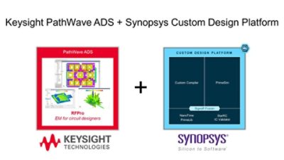
Cedric Pujol, Product Manager, Keysight Technologies and Damian Roberts, Sr. Staff AE, 17│į╣Ž, demonstrate the unified solution for full flow RFIC design and show how designers are achieving faster layout and design closure with this integrated flow.
In part 2 of this video series, Shabbir Batterywala, 17│į╣Ž Scientist, shows how layout designers create complex parameterized custom layout structures in an easy-to-use graphical environment, without any programming.
In part 1 of this video series, Shabbir Batterywala, 17│į╣Ž Scientist, will show how layout designers can create parameterized custom layout structures in an easy-to-use graphical environment, without any programming.

In this 7th video of the series, Kai Wang, Director of Engineering at 17│į╣Ž, discusses in-design electrical analysis, and why it is critical to use signoff engines to check and fix resistance, capacitance and electromigration issues during layout.

In this 6th video of the series, Kai Wang, Director of Engineering at 17│į╣Ž, discusses methodology innovation in early electrical analysis to reduce iterations, and bringing signoff tools into the design process to speed up analog design closure.

In this 5th video of the series, Kai Wang, Director of Engineering at 17│į╣Ž, explains the need of Monte Carlo to improve yield, and how designers use advanced features like variation scoping and sigma amplification to avoid costly MC simulations.

In this 4th video of the series, Kai Wang, Director of Engineering at 17│į╣Ž, explains how device aging effects are more prominent because of stringent operating conditions, and how 17│į╣Ž robust aging analysis helps in design for reliability.

In this 3rd video of the series, Kai Wang, Director of Engineering at 17│į╣Ž, introduces circuit checks and explains how designers avoid wasted simulation time by finding design and performance problems automatically in advance.

In this 2nd video of the series, Kai Wang, Director of Engineering at 17│į╣Ž, introduces analog fault simulation and explains how 17│į╣Ž TestMAX? CustomFault? enables full-chip functional safety and test coverage analysis.

In part I of this video series, Kai Wang, Director of Engineering at 17│į╣Ž, will highlight key technologies in 17│į╣Ž Custom Design Platform to address reliability challenges across the analog design cycle.

Soni Kapoor, Sr. Technical Marketing Manager in 17│į╣ŽĪ» Custom Design Group, discusses Custom Compiler? Visually-Assisted Layout Automation technology in action as we finish an analog block in one hour that took three days to complete the old-fashioned way.

Neel Gopalan, Principal Applications Engineer in 17│į╣Ž' Custom Design Group, discusses how Custom CompilerĪ»s Quick Start Kits (QSKs) help designers accelerate layout and reduce design iterations.

Michael Lynch, R&D Director for SerDes IP in 17│į╣Ž' 17│į╣Ž Group, discusses how using Custom Compiler? Partial Layout Extraction flow significantly reduces design iterations via early electrical analysis.

Custom Compiler? solution speeds layout creation with user-guided routing and reusable templates.

Custom Compiler? design and layout solution reduces design closure time with signoff-quality early electrical analysis.


